Photonic neuromorphic computing
As artificial intelligence (AI) continues its rapid evolution—driven by groundbreaking developments in deep learning and the relentless pursuit of artificial general intelligence (AGI)—the scale and complexity of computational tasks have surged to unprecedented levels. These emerging challenges stretch the capabilities of conventional electronic computing architectures, which are now increasingly restrained by fundamental physical limits. Moore’s Law, once a dependable harbinger of exponential increases in transistor density and computing power, is now approaching its limits as device miniaturization nears the atomic scale. Simultaneously, escalating power consumption and thermal dissipation further impede performance improvements, underscoring the critical need for alternative computing paradigms.
Photonic computing has emerged as a particularly promising solution. By leveraging optical signals rather than electronic ones for both data processing and transmission, this approach harnesses the intrinsic advantages of light—namely, high propagation speeds, low energy requirements, and exceptional parallelism—to deliver breakthroughs in both speed and efficiency. Advanced techniques such as wavelength-division and spatial-division multiplexing enable the simultaneous processing of multiple optical channels, dramatically increasing computational throughput. Moreover, the inherently low latency of photonic systems renders them exceptionally well-suited for real-time data processing and large-scale parallel computing applications. As the demands of computational workloads continue to escalate, photonic computing represents a transformative shift that holds the potential to redefine the future of high-performance computing.
The all-optical neural network (ONN), built on nanophotonic circuits, represents a major milestone in photonic computing for deep learning applications. This architecture employs optical interference units (OIUs) to execute linear matrix operations and optical nonlinear units (ONUs) to implement activation functions. The researchers developed a programmable nanophotonic processor on silicon photonic integrated circuits (SPICs), featuring an array of 56 Mach–Zehnder interferometers (MZIs) to perform efficient matrix multiplications. Notably, the ONN achieved an accuracy of 76.7% on a vowel recognition task¹.
The diffractive deep neural network (D²NN) is a groundbreaking architecture that leverages multiple passive diffractive layers to perform deep learning tasks through light diffraction. Each layer incorporates a precisely engineered phase mask to modulate the propagation of optical signals, enabling rapid linear transformations and feature extraction with minimal energy consumption. A five-layer D²NN demonstrated classification accuracies of 91.75% on the MNIST dataset and 86.6% on Fashion-MNIST², closely matching the performance of conventional electronic neural networks.
Optical convolution accelerators (CAs) enhance the performance of convolutional neural networks (CNNs), which are critical for image recognition, by integrating Kerr microcomb sources, multi-wavelength channels, and electro‑optic modulators. Leveraging optical signal modulation, delay, and weighted summation, these accelerators efficiently execute the sliding‑window operations of convolutional kernels. One such optical CA achieves 88% accuracy on the MNIST dataset, processes images containing up to 250,000 pixels, and operates at an impressive rate of 11 trillion operations per second (TOPS)³.
Another vital aspect of photonic neuromorphic computing is the implementation of optical nonlinear activation functions, which completes the development of an end-to-end integrated photonic deep neural network (PDNN). The PDNN utilizes on-chip optoelectronic hybrid technology to process input data optically while employing micro-ring modulators (MRMs) to realize nonlinear activation functions. This design removes the need for analog-to-digital conversion and large memory modules, yielding significant gains in both speed and energy efficiency. The PDNN achieves classification times as low as 570 picoseconds, a computational density of 3.5 TOPS/mm², and an energy consumption of just 345 femtojoules per operation⁴, underscoring the enormous potential of optical computing for efficient image classification and other computationally demanding tasks.
Chiplet-based photonic neuromorphic computing holds promise for overcoming the challenges of noise accumulation and hardware imperfections in existing systems. A notable example is the “Taichi” chip, which integrates interferometric and diffractive designs through a distributed computing strategy. This approach enables a highly scalable and flexible framework built on a shallow-wide network architecture. The chiplet demonstrated its capability by performing 1,623-class image classification on the Omniglot dataset, achieving a test accuracy of 91.89% and an energy efficiency of 160 tera operations per second per watt (TOPS/W)⁵. Furthermore, it has been successfully applied to content generation tasks—including stylized image synthesis and music generation—highlighting its potential in multimodal AI applications.

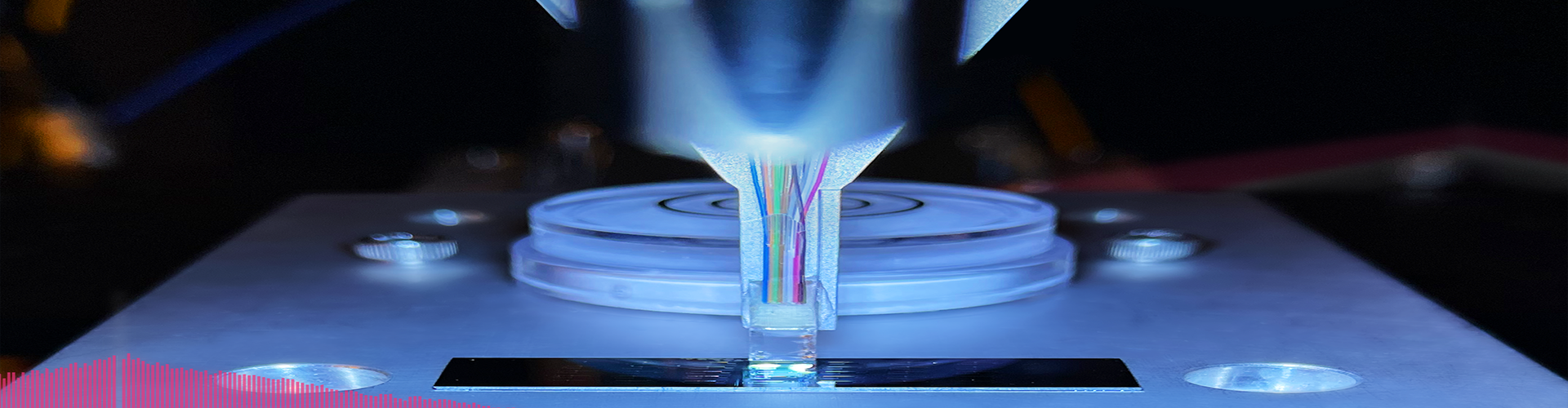
Fig. 1 | Photonic-integrated EO-DiAL
Our research centers on a system‑level thin‑film lithium niobate (TFLN) platform that leverages the electro‑optic (Pockels) effect and its inherent scalability to achieve high‑speed data encoding and computation across both electrical and optical domains—addressing the inherent limitations of conventional electronic and photonic computing architectures. In Fig. 1, we present a general electro‑optic digital‑to‑analog link (EO‑DiAL)⁶ enabled by foundry‑based lithium niobate nanophotonics, which achieves information rates of up to 186 Gbit/s. This system overcomes the digital‑to‑analog conversion challenge in photonic computing by delivering high‑fidelity MNIST encoding with an energy consumption of only 0.058 pJ/bit. In Fig. 2, we demonstrate a scalable TFLN computing accelerator for matrix‑vector multiplication (MVM)⁷, realized by integrating high‑performance electro‑optic devices into an optimized large‑scale photonic circuit. This accelerator achieves photonic computation speeds of up to 1.36 TOPS while consuming just 0.057 pJ per operation, thereby surmounting current speed and power constraints in state‑of‑the‑art computing systems and establishing the most advanced TFLN electro‑optic computing platform to date. Our work also encompasses advancements in photonic computing and optical interconnects, aiming to realize large‑scale, high‑precision AI platforms that will serve as critical enablers for applications in autonomous driving, medical imaging, artificial intelligence, and beyond.

Fig. 2 | Photonic computing accelerator on thin-film lithium niobate
1. Deep learning with coherent nanophotonic circuits | Nature Photonics. https://www.nature.com/articles/nphoton.2017.93.
2. Lin, X. et al. All-optical machine learning using diffractive deep neural networks. Science 361, 1004–1008 (2018).
3. Xu, X. et al. 11 TOPS photonic convolutional accelerator for optical neural networks. Nature 589, 44–51 (2021).
4. Ashtiani, F., Geers, A. J. & Aflatouni, F. An on-chip photonic deep neural network for image classification. Nature 606, 501–506 (2022).
5. Xu, Z. et al. Large-scale photonic chiplet Taichi empowers 160-TOPS/W artificial general intelligence. Science 384, 202–209 (2024).
6. Song, Y. et al. Integrated electro-optic digital-to-analog link for efficient computing and arbitrary waveform generation.
7. Hu, Y. et al. Integrated lithium niobate photonic computing circuit based on efficient and high-speed electro-optic conversion.